
The expensive part of an AI system is increasingly the memory around the accelerator, not just the accelerator itself. Samsung’s newly expanded collaboration with ASML is therefore worth watching even though it will not put a new stick of RAM in anyone’s PC this year.
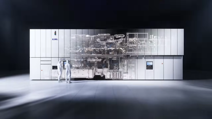
The companies say Samsung intends to use ASML’s High-NA EUV lithography in high-volume DRAM manufacturing by 2028. At the same time, Samsung is joining an industry effort around a larger photomask format for the machines. Taken together, those are attempts to make the next hard stage of memory scaling more manufacturable—not a promise that every future laptop suddenly gets cheap, enormous memory.
That distinction matters. Semiconductor roadmaps are full of dates that depend on yields, materials, mask infrastructure and demand. Samsung’s September 8 announcement is a declared plan, not evidence of production today. But it is concrete enough to change the conversation from “will High-NA EUV ever reach memory?” to “can Samsung make it work at useful scale?”
What Samsung has actually committed to
Samsung and ASML say they are deepening work on High Numerical Aperture extreme-ultraviolet lithography, with a stated goal of applying it to future high-volume DRAM production by 2028. Samsung describes that as an industry first.
The other half of the news is easier to overlook and may be just as important: photomasks. A mask is the patterned template used to transfer circuitry onto a wafer. Samsung is joining an initiative to develop a 12-inch platform for High-NA EUV, replacing a 6-inch format the industry has used for decades.
| The change | Why it matters |
|---|---|
| Higher numerical aperture | Finer patterning can reduce the number of steps needed for demanding structures. |
| 12-inch mask platform | Designed to ease High-NA EUV’s exposure-field and stitching constraints. |
| 2028 DRAM target | Sets a date against which Samsung’s manufacturing progress can be judged. |
| High-volume production | Much harder—and more meaningful—than demonstrating a lab process. |
Samsung says the bigger mask work is intended to lift productivity, lower manufacturing cost and remove stitching constraints. Seoul Economic Daily adds useful context: High-NA EUV systems have a smaller exposure field than conventional EUV, which is why the industry is pursuing a larger mask architecture rather than treating the scanner as a drop-in replacement.
Why memory, rather than just smaller logic chips, is the interesting target
High-NA EUV is often discussed as a tool for leading-edge processors. Bringing it to DRAM changes the audience. DRAM density and efficiency now influence everything from a phone’s multitasking headroom to the amount of high-bandwidth memory an AI accelerator can carry.
That does not make a 2028 lithography deployment a direct prediction of retail RAM prices. Memory pricing also follows capacity additions, product mix, inventory cycles and the allocation of leading-edge output to server and AI customers. Still, the manufacturing direction is relevant to consumers because memory pressure has already escaped the data center. As we noted in our look at Apple’s widening device price increases, expensive memory and storage inputs eventually work their way into mainstream hardware.
TrendForce frames the competitive angle clearly: Samsung and SK hynix both have 2028 High-NA EUV ambitions for DRAM, while Micron has been more restrained publicly about its own timeline. Samsung’s announcement does not settle that race, but it gives the company a visible milestone in an area where HBM, advanced DRAM and AI infrastructure are now tightly connected.
Bigger masks are a practical bet, not a glamorous one
The compelling detail here is not that the masks double from six inches to 12. It is that High-NA EUV needs an ecosystem around the scanner: masks, inspection, materials, process flows and the routines that turn a promising exposure into repeatable yield.
Samsung says a larger mask format should help fully exploit High-NA EUV. Independent reporting similarly points to fewer stitching compromises and better throughput as the rationale. Those are factory economics, but factory economics are where ambitious node claims either become available products or remain excellent slides.
There is also a healthy caveat. A larger mask is not a magic coupon for cheap chips. New equipment and process changes are expensive, qualification takes time, and early production can carry a cost penalty before learning improves yields. The announcement gives Samsung a roadmap; it does not reveal product-level DRAM densities, power figures, yields, customer qualification or pricing.
What to watch between now and 2028
The next meaningful evidence will be less theatrical than a keynote: mask-platform progress, tool installation, process demonstrations, yield disclosures and a named DRAM generation. A claim that High-NA EUV is “ready” matters only if it is accompanied by a credible path to volume production.
For builders and buyers of AI hardware, the broader lesson is that memory is becoming a primary technology battleground. Faster accelerators without enough efficient memory are badly balanced systems. Samsung’s ASML plan is a bet that lithography can keep memory density and manufacturing complexity moving in the right direction before that imbalance becomes more painful.
Bottom line
Samsung has not announced a new consumer memory product. It has announced a manufacturing target with real strategic weight: High-NA EUV DRAM production by 2028, supported by a shift to larger masks.
The prudent reading is not that cheaper RAM is around the corner. It is that one of the world’s biggest memory makers is putting a date on the next expensive, difficult toolset for AI-era memory. If Samsung meets it with healthy yields, the benefits will show up downstream—in denser memory, more capable AI systems and, eventually, hardware whose memory bill is a little less brutal. Until then, it is a promising plan that still has to earn its way through the fab.